vCard
vCard
 Homemade by CVG
 My Homemade Apps
 Thingiverse
 Strava
XT0F-003 - my first WSN node
In 2012 I was introduced to Wireless Sensor Networks (WSN) and it didn’t take too long before I fell in love with this (relatively) new technology. As it will be the topic of my upcoming master’s thesis, I felt obliged to at least once implement and maintain a WSN from the ground up.
At the lowest level there are of course … the motes.
Design
Being my first sensor node and even my first actual electronics design, I chose two simple sensors: a light sensor (TSL252R) and a temperature sensor (AD22103). Wireless connectivity, using the Zigbee protocol stack, was implemented using the very complete XBee module. An ATMEGA328 was added to steer all functionality. Finally, a 1700mAh LIPO battery should allow the node to run at least 5 days - which was the initial goal when taking the project to the OpenGarage ↗ Village at OHM2013.
Bill Of Material
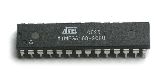
- 1 ATMEGA328 with socket
- 1 XBee with break-out board and headers
- 1 TSL252R light sensor
- 1 AD22103 temperature sensor
- 1 MCP1700 3V regulated power supply
- 1 1700mAh LIPO battery ↗ with additional female connector
- 4 5mm LEDs for visual verification of functioning
- 1 pushbutton
- 5 100nF capacitors
- 4 resistors: 2 100Ω, 1 1KΩ, 1 10KΩ
Software
Details about the software can be found on each of the components’ own pages. All source code is available in my public embedded GitHub repository ↗. The main.c, using the other reusable components’ code from that repository, is located in the xt0f-003 ↗ directory.
The software has a loop that gets all sensor values and then puts everything to sleep for 59 seconds.
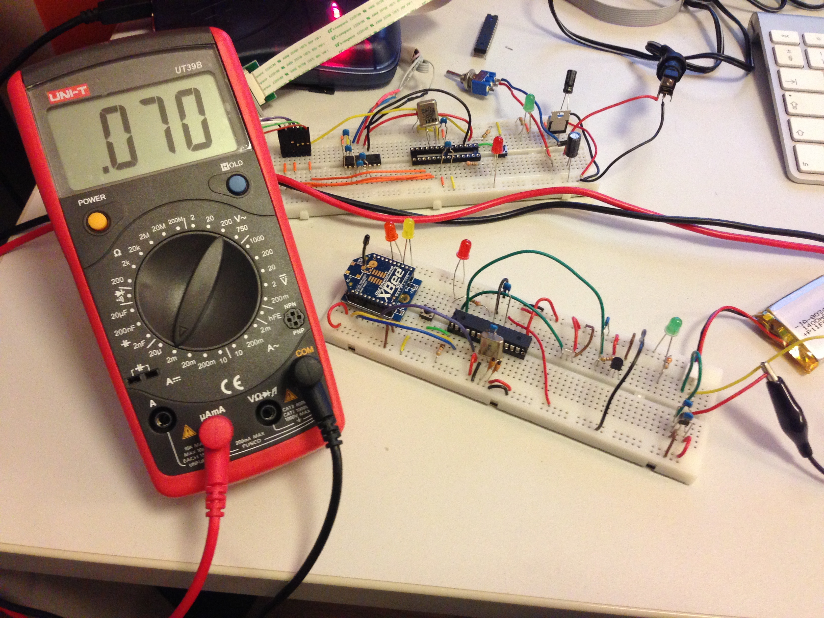
Without power management, the mote requires about 70mA, which would result in 20 hours of operation (1400/70=20). After putting the XBee module to sleep I got it down to 10mA while asleep and still 70mA when active, which would give me roughly an average current of 11mA or about 5 days.
After I finally got my head around the power management of the ATMEGA itself, the mote only required 0.07mA (or 70μA), resulting in an average current of 1.24mA which theoretically would make the battery last about 45 days :-)
Status
Currently the software for the node is functional, but the readings are off. The power supply level reading is way off and the sensor readings seem to be consistently too low. I think it has to do with the way I’m reading values from the ADC, which is implemented in the generic AVR code ↗. So I’ll try to solve it there. Once this is fixed, the node will probably operate as expected.
Hardware
This remainder of this page focuses on the hardware design. Below are the components design and the different board revisions, each with goals and considerations.
Circuit Design
The circuit is in fact a collection of modules: a 3.3V regulated power supply, the XBee module, 2 basic sensor modules and the central ATMEGA controlling module. This is reflected in the circuit design below:
Operational on a breadboard, it looks like this …
Revision 1 - aka the OHM revision
With the first implementation I of course tried to get the thing of the breadboard and onto a through-holes board. Although not my main focus, I did try to layout the board as compact as possible.
At this point I was using generic through-hole boards, no nice PCBs yet. Components go on one side and connections were made using a solid wire, following the 2 dimensional grid of holes. Sometimes it was not possible to layout all the connections without crossings. Those were then created using solid wires with their coating still on. Those connections are shown in orange on the circuit.
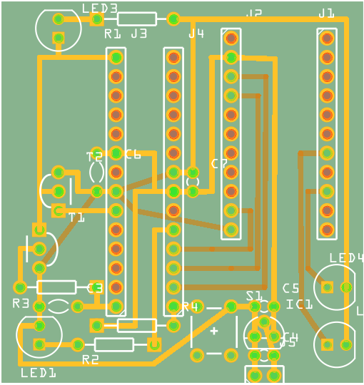
Status: Implemented
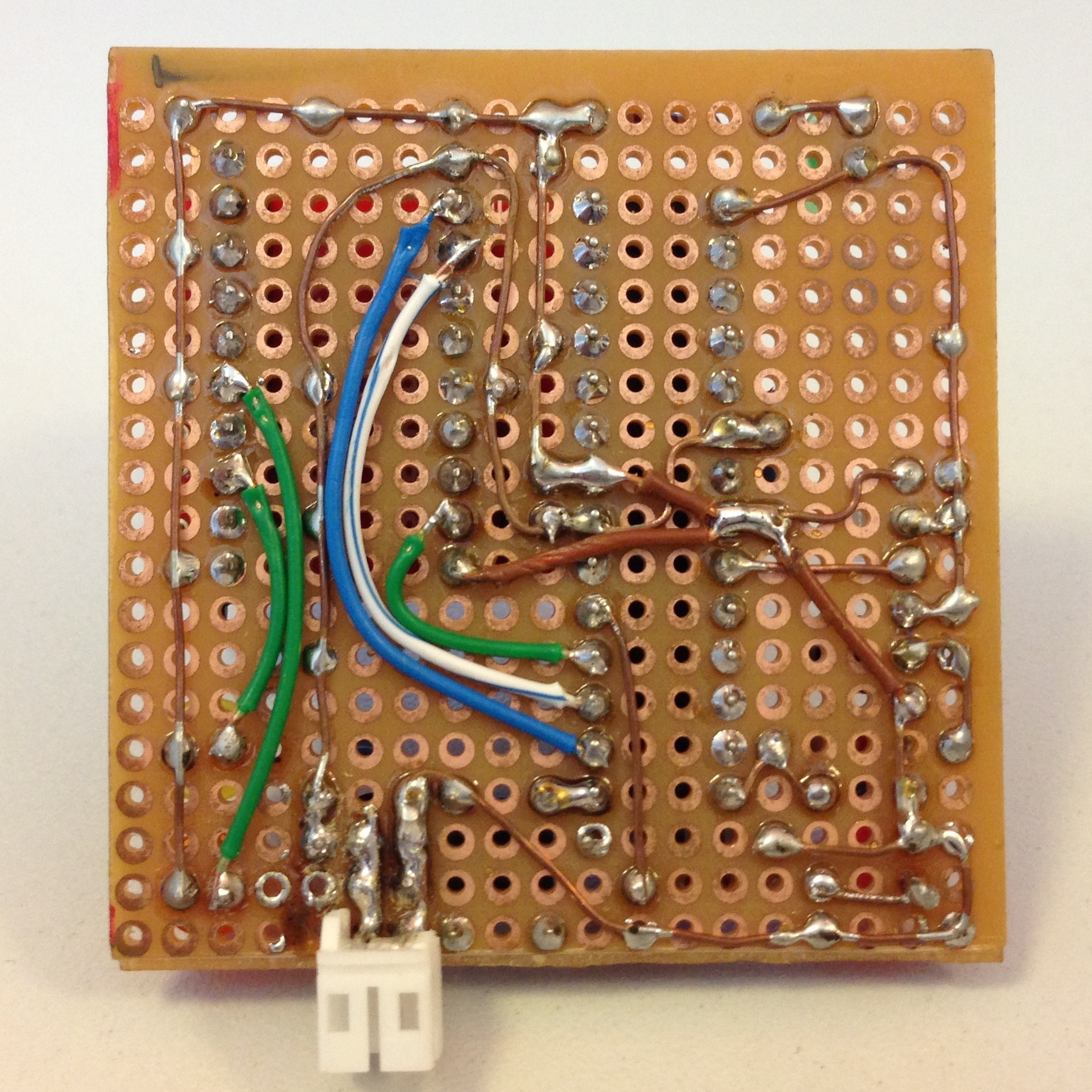
While (finally) documenting all this, I noticed that I had made an error in the implementation. Apparently, I wrongly connected the pull-up resistor to GND in stead of to 3.3V. But, as I hadn’t connected it to the RESET pin of the ATMEGA, the pin was floating, which apparently is good enough. The reset button did function as expected, so I didn’t notice it. If you look carefully at the picture of the bottom of the board, you could spot the missing connection from the pull-up resistor and the RESET pin :-)
Revision 2 - aka the Manu revision
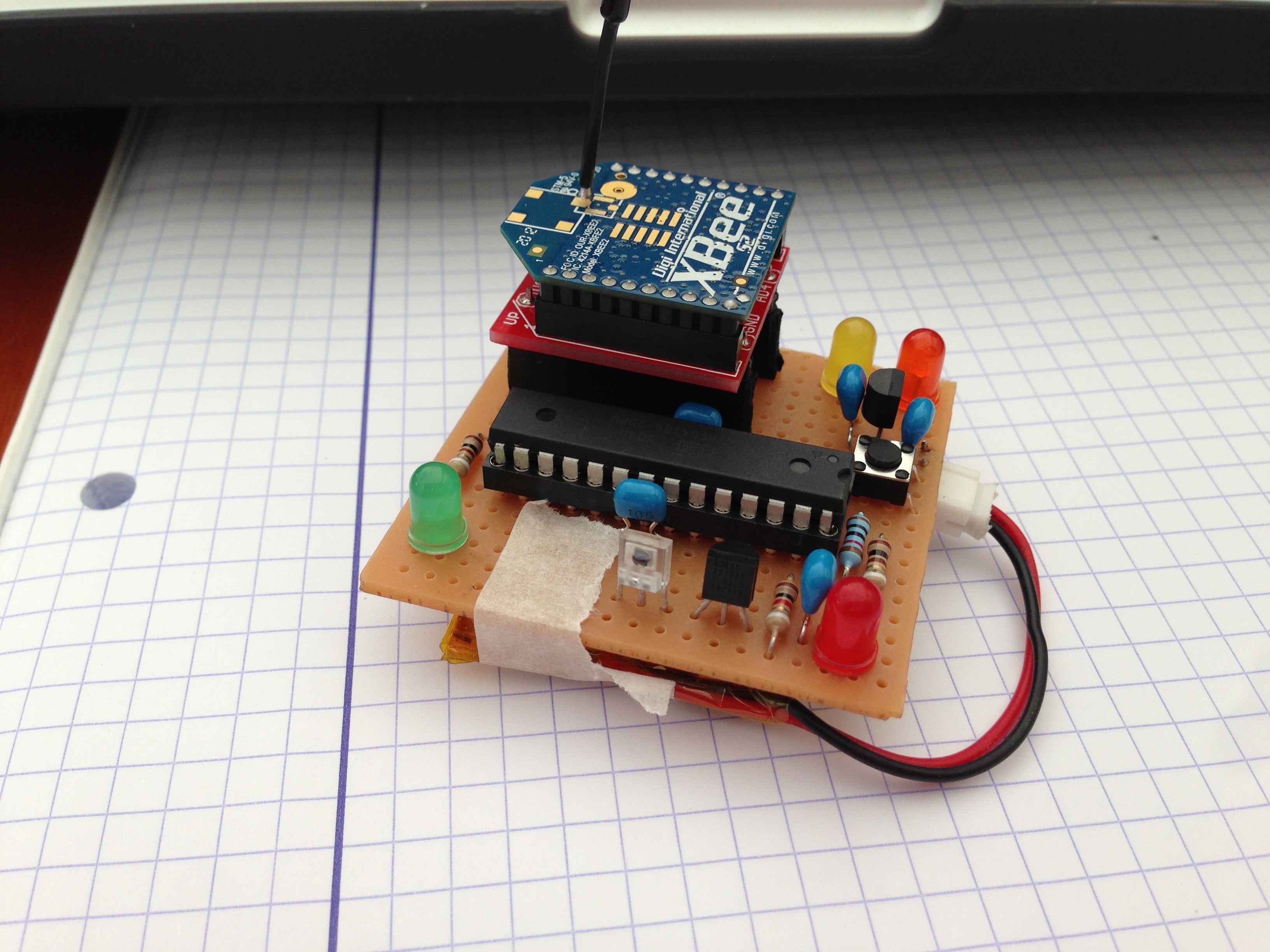
As soon as the first revision was ready, it was clear that the overall form-factor was too big. This was mainly due to the fact that I didn’t want my XBee module to be attached permanently. The stack consisting of a female header, the break-out board with male and female headers and the XBee itself was standing tall like a skyscraper.
Manu, a good friend of mine, came up with the idea to reduce the footprint by splitting the board into two sections, of which one could be mounted above the other at the same height as the XBee. Adding all LEDs and sensors to that secondary board, would also bring all external components to the same level, which would allow for a better casing design.
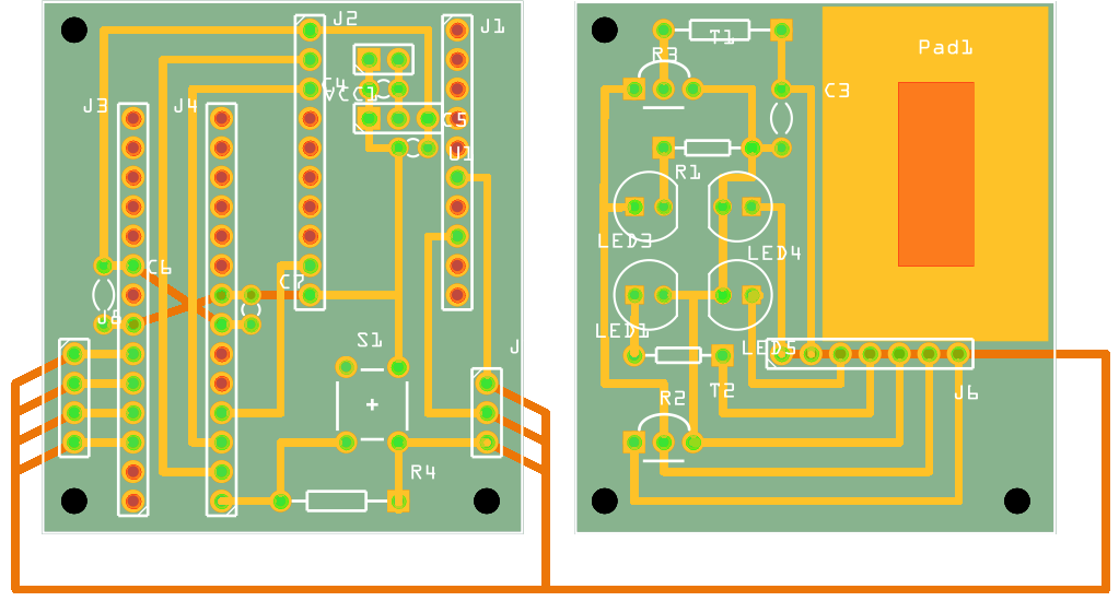
The two board are connected using seven wires, connected on both boards to headers. The pad shows the part that could be cut from the top board to make room for the top of the XBee module.
A nice improvement on this revision is the use of the space underneath the XBee module. The regulated power supply fits nicely, something I hadn’t thought of in the first revision. Both board also show 3 holes to mount them on top of each other using threaded rods and nuts.
But …
Status: Not implemented.
Although a very good idea, the design didn’t live up to the expectations and while designing it, I came up with a variation on it and therefore I abandoned this design and started revision 3.
Revision 3 - aka the Modular Cube revision
While designing revision 2, I came up with a different approach, which puts the top board orthogonal to the base board and connects the two board using a pair of male and female headers. A bit like a plug-in board for the MCU’s base board.
This idea continued to grow and evolved towards a multi-board construction around the XBee stack.